
Shangjian deepens its efforts in advanced process and packaging inspection market, and expands domestic and overseas development of the three major businesses
Semiconductor Inspection Commercial Technology stated at its 20th anniversary event that the company is committed to deepening advanced processes and advanced packaging area material analysis (MA) services, and actively expanding global market layout, including covering major semiconductor industries such as Taiwan, China, Japan, and the United States, and is determined to become an important partner in key inspection and analysis for global semiconductor research and development innovation. Looking ahead, the company will strengthen the expansion of three major business dynamics through the advantages of material analysis (MA) and AI sub-testing and analysis technology, "Amy Generation Process Material Analysis", "Silicon Photonic Testing and Light-Decayed Light-Drained Light Analysis", and "AI Customer Area".
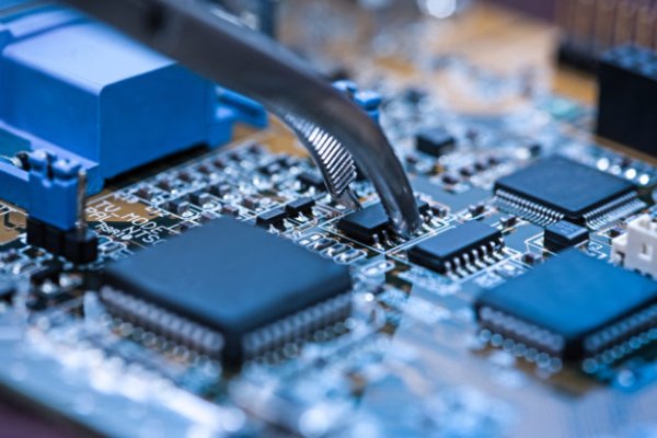
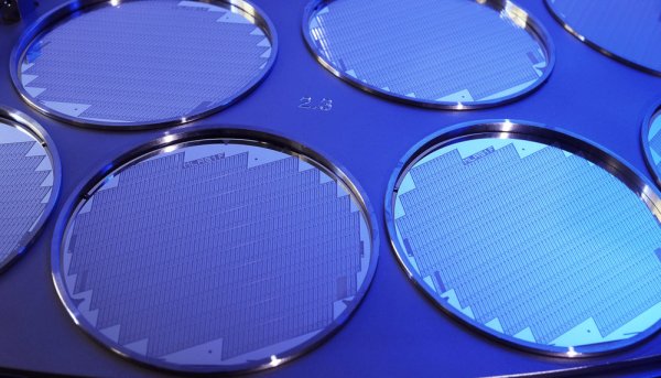
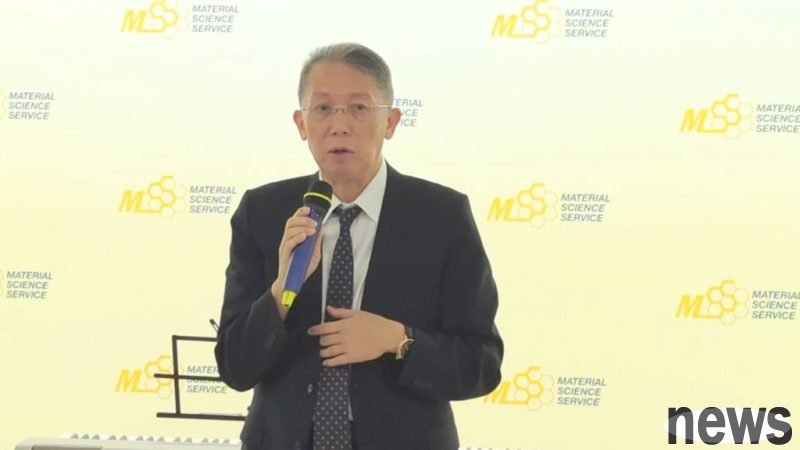
文版 said that with the booming development of AI applications, it has ignited the global semiconductor technology innovation competition, promoting the integration of higher speed, low power consumption and high density of wafer design, and has officially entered the Amy (0.1 nanometer) generation, which is comparable to the penetrating electronic microscope (TEM) technology that has been relied on in previous nano-level processes.
文 pointed out that the doorsteps of Amy Generation have greatly improved in the analysis resolution and stability. Only with the experimental facilities with spherical aberration correction TEM and extremely low interference environments can we meet the requirements of advanced process research and development verification. To this end, the SAC-TEM Center building has created a new generation of high-level SAC-TEM Center, which adopts a single floor independent vibration-proof foundation and a three-layer steel bone shock-resistant structure design, providing the highest specification lens operation conditions, and the SAC has key technologies such as low-temperature ALD and ultra-thin trial film preparation, laying the foundation for the next ten years of material analysis competition, and is the 20-year advance positioning of the semiconductor gold.
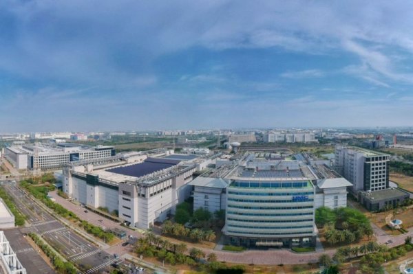
In addition, in order to master the global semiconductor industry regionalization trend, we will launch international operation and expand international operations, and actively build four locations in Taiwan, China, Japan and the United States, comprehensively enhance global service coverage and expand new customer acquisition machines. Especially this year, as we enter the 20th anniversary, for the first year of the globalization of the market, it will include the Zhubei operation site to carry out multiple upgrades and upgrades, and set up the Amy Generation 1.0-nanometer to 1.4-nanometer material analysis area, AI area, silicon photon positioning analysis center, and the Zhubei SAC-TEM Center new factory that will be launched to enhance the overall experiment and detection energy.
Shanghai has emphasized that in order to meet global customer needs, it will accelerate the overseas experiment room layout. Its American subsidiary MSS USA CORP Silicon Valley experiment room has been officially launched, focusing on serving semiconductor manufacturers and its suppliers, and extending to other industries that have high demand for advanced material analysis, including international leading technology companies, new ventures, research institutions and advanced process-related companies, all of which are future potential customers.
In addition, Japan is also expected to invest in the ranks of people and operate in September 2025 to further expand the global material analysis capacity. As global operation points are gradually in place, the detection and analysis capacity is simultaneously improved with local service capabilities, and the competitive advantages of the international semiconductor material analysis market will be further strengthened. In the future, we will continue to integrate R&D resources, deepen high-level testing technology, and work with global customers toward higher-level technology generations, jointly create a new chapter of sustainable growth.