
Telecom 3D vertical stacking and packaging solutions to solve double challenges in AI face
With the booming development of AI applications, from smartphones, Internet devices to automatic driving, the market demand for high-performance, low-power, and small-scale chips is becoming increasingly demanding. Global GRF Foundry Corporation analyzed the double-frequency challenges facing edge AI at Semicon Taiwan's lecture activities, and revealed its positive transformation. With advanced 3D vertical stacking and packaging solutions, it breaks through the physical limitations of traditional 2D plane design and leads the semiconductor industry to a new element.
Wang Yuping, president of the Technology Development Director of the Advanced Packaging Department of Telecom, pointed out that the Edge AI device is in an interesting two difficult dilemma. On the one hand, when the device needs to call the cloud server's powerful computing power for co-operation (Call for help), it requires extremely high external wireless communication bandwidth. On the other hand, when an AI agent (Agent) within the device performs complex real-time computing and decisions, the processor and the memory also requires a very high intra-to-date data transmission bandwidth.
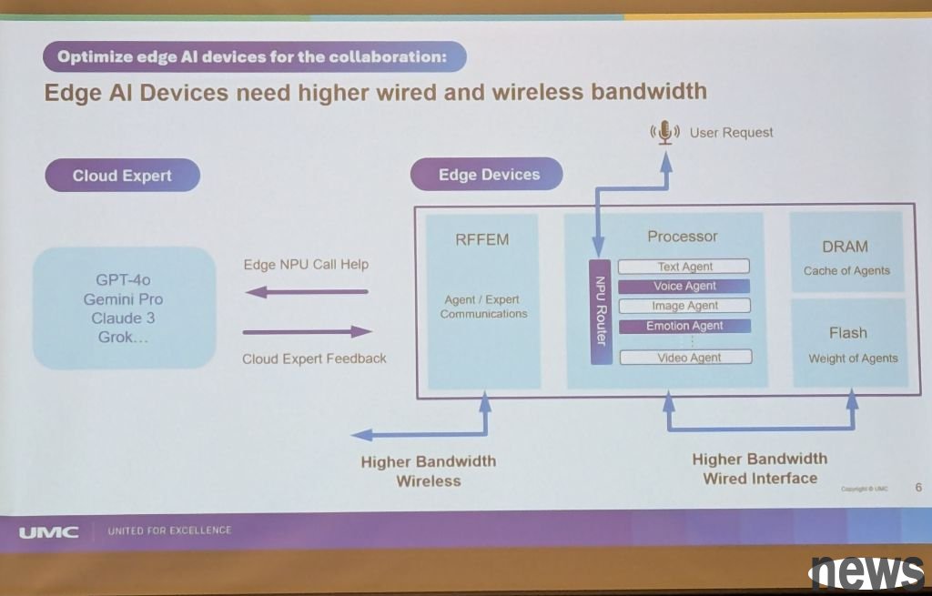
Due to this wide demand for internal and external collisions, this has created a huge challenge for the traditional 2D planar chip design. To improve external communication capabilities, a RF Front-end Module must be added, but this will cause the chip surface to expand rapidly. Similarly, in order to enhance internal computing efficiency, AI agents need to use a large amount of DRAM as cache and Flash storage rights. These components each occupy space on traditional PCB circuit boards, which not only reduces overall power consumption and physical limitations, but also limits further improvements in performance. Traditional design thinking has already touched the double ceiling of physics and cost.
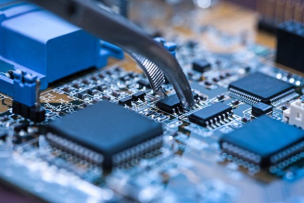
Wang Yuping said that in order to solve this dilemma, Telecom has proposed a fundamental solution, that is, to move from 2D to 3D. He metaphorically said that the shortest distance between two points in the universe may not be a straight line, but a space is folded up. This concept perfectly expounds the core advantages of 3D vertical stacking technology. By stacking and connecting different functional wafers (such as processors, memory, radio modules) vertically, it can achieve extreme size reduction. This is compared to expanding all components on the same plane. The vertical stacking can greatly reduce the overall volume of the wafer, meeting the strict requirements of the edge device for lightness, shortness.
In addition, there are shorter transmission paths, such that the transmission distance of the signal in the vertical direction is much shorter than the radial distance on the plane, which directly leads to lower delays and higher transmission speeds. Also, the excellent energy efficiency, depending on the shortening of transmission paths, the signal consumption and driving required power consumption is significantly reduced, thereby greatly improving the overall energy efficiency and extending the battery life of the edge device.
In this regard, Wang Yuping explained the module structure edge AI chip of the connection, which dissolves the complex system into four key "Building Blocks", power management chips (PMICs), radio front-end modules, processors and memory, and integrates them efficiently through 3D stacking technology. Behind the above scenario is the deep special process technology burden of the Internet. In particular, Connecticut is transforming its unique special technology into a scaled advanced packaging solution.
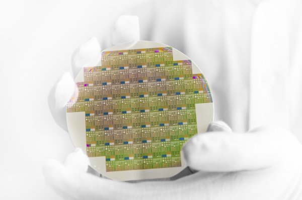
Wang Yuping emphasized that in the "Silicon Interposer" technology, the power supply not only provides pure silicon interposer, but also further integrates deep slot capacitors, providing excellent signal and power integrity for high-frequency wide computing. Secondly, for the demand for different quality integration, the "TSV-last" technology of the Electric Power Company, Wafer Thinning and Hybrid Bonding technology enable it to receive wafers from customers or third parties (such as DRAM manufacturers) and conduct precise vertical integration in the Electric Power Company's factory. At present, Connect has successfully combined the external DRAM memory crystal with its own logical crystal to create an extremely cost-effective AI recommendation engine (Inference Engine), which fully verifies its technical capabilities.
Wang Yuping emphasized that the system-level integration of Edge AI is extremely complex and requires the cooperation of the entire ecosystem. Telecom knows that this technical change cannot be completed by just one's own efforts. Therefore, Joint Power has launched in-depth cooperation with EDA analog software suppliers, equipment manufacturers and rear-end packaging testing (OSAT) partners to jointly create a complete and efficient solution platform.