
Intel has fully put into production the Intel 18A process, and the new architecture covers the client and server markets to fulfill its promise

Chip manufacturer Intel announced full production of the Intel 18A process, including client Panther Lake series and server Clearwater Forest processors, which will use the first 2-nanometer process node developed and manufactured in the United States. It will be manufactured at the Fab52 fab in Arizona. Its products will be released later to fulfill its previous emphasis on Intel 18A process in 2025. Commitment to mass production in the second half of the year.
Panther Lake built on Intel 18A process can expand AI PC performance
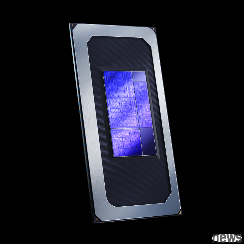
The new generation of client Intel Core Ultra processors (Series 3), code-named Panther Lake, is Intel’s first product to use the Intel 18A process. This technology is hailed as the most advanced semiconductor process technology developed and manufactured in the United States. This represents Intel’s achievement of a key milestone in strengthening U.S. technology and manufacturing leadership and building a resilient semiconductor supply chain.
 ▲ Intel manufacturing technicians hold Intel Core Ultra processors (Series 3) (codenamed Panther Lake) manufactured using the Intel 18A process.
Intel stated that Intel Core Ultra processors (Series 3) are expected to begin shipping later in 2025 and are expected to enter the market in January 2026. Panther Lake is the first client system-on-chip (SoC) using Intel's 18A process and targets a wide range of markets, including consumer and commercial AI PCs, gaming devices and edge computing solutions.
Panther Lake adopts a scalable multi-chiplet architecture, providing partners with unprecedented flexibility in different form factors, application fields, and prices. In terms of performance, Panther Lake is designed to have Lunar Lake-level energy efficiency and Arrow Lake-level performance.
In terms of major performance improvements and features, Panther Lake is equipped with up to 16 new performance cores (P-cores) and efficiency cores (E-cores). The CPU performance is improved by more than 50% compared to the previous generation. In addition, the new Intel Arc GPU with up to 12 Xe cores also improves graphics performance by more than 50% compared to the previous generation. The balanced XPU design can achieve a higher level of AI acceleration, with platform computing performance up to 180 TOPS (180 trillion operations per second).
 ▲ PantherLake, Intel’s first product using the Intel 18A process.
In addition to the personal computer market, Panther Lake will also extend to edge computing applications, such as robotics. Customers can leverage the new Intel Robotics AI software suite and reference development version to quickly develop cost-effective robots using Panther Lake's computing and AI perception capabilities. Panther Lake will enter mass production starting in 2025, with the first products expected to ship before the end of the year.
Clearwater Forest brings efficiency and scale to modern data centersIn addition to the client field, Intel also announced the release of the first server processor Xeon 6+ using the Intel 18A process in the server field, code-named Clearwater Forest. This new generation of efficiency core processor is hailed as Intel's most efficient server processor to date and is expected to be officially launched in the first half of 2026.
 ▲ Intel Intel will showcase the Intel Xeon 6+ processor (codenamed Clearwater Forest) manufactured using the Intel 18A process at the 2025 Intel Technology Tour.
Intel pointed out that Clearwater Forest is tailor-made for hyperscale data centers, cloud service providers and telecom operators, aiming to help enterprises expand workloads, reduce energy costs, and promote smarter service operations. The main features of Clearwater Forest include up to 288 efficient cores, a 17% increase in instructions per cycle (IPC) over the previous generation, and significant improvements in density, throughput and energy efficiency.
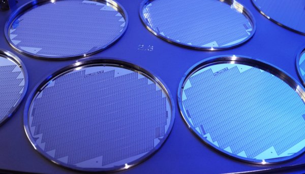
Intel 18A is the first 2nm-level process node developed and manufactured in the United StatesAs for the Intel 18A used in the Panther Lake and Clearwater Forest product lines this time, Intel emphasized that this is the first 2-nanometer process node developed and manufactured in the United States, and it is a symbol of American technology setting new industry standards. Compared with the previous generation Intel 3 process, Intel 18A’s performance per watt is increased by up to 15%, and the chip density is increased by 30%. This process node has completed R&D and manufacturing verification at Intel's Oregon base. It has now been put into early production and is entering the mass production stage in Arizona..
 ▲Manufacturing technicians at Intel’s new Fab 52 fab in Chandler, Arizona.
Intel explained the two key innovative technologies of the Intel 18A process. The first is the application of RibbonFET, which is the first new transistor architecture introduced by Intel in more than ten years. It can achieve better expansion and more efficient switching, effectively improving performance and energy efficiency. PowerVia is also used, an innovative chip back-side power supply technology to improve the efficiency of current transmission and signal transmission.
In addition, through Intel's advanced packaging and 3D chip stacking technology Foveros, multiple chip modules can be stacked and integrated into advanced single-chip (SoC) designs, thereby providing higher flexibility, scalability and performance at the system level. Intel 18A will form the technology foundation for at least three generations of Intel client and server products.
Arizona Fab 52 will become a key engine built in the United StatesIncluding Panther Lake, Clearwater Forest and multiple generations of products using the Intel 18A process, all are produced at the state-of-the-art Fab 52 fab in Chandler, Arizona. Fab 52 is Intel's fifth high-volume production fab at its Ocotillo campus in Arizona, tasked with producing the most advanced logic chips in the United States.
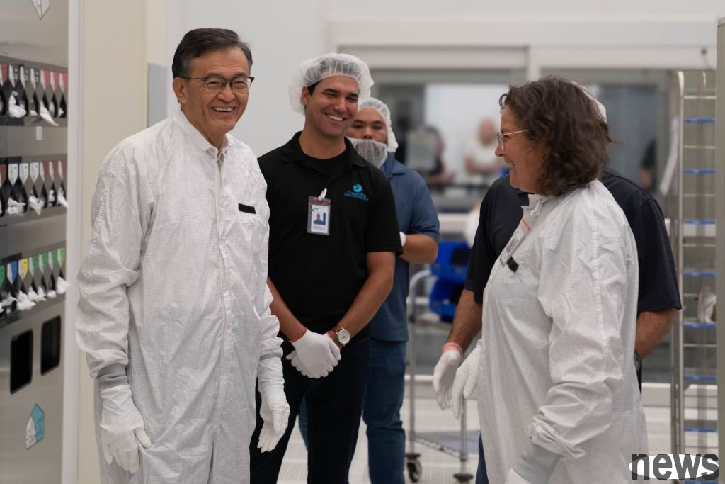 ▲ Intel CEO Liwu Chen wore a clean room protective clothing and visited Intel's Fab52 fab in Chandler, Arizona.
The construction of Fab 52 is an important part of Intel's $100 billion investment to expand its U.S. operations. With advanced R&D and production capabilities in Oregon, large-scale manufacturing in Arizona, and packaging operations in New Mexico, Intel is uniquely positioned to support key national priorities and provide strategic capacity to Intel's wafer customers. Fab 52 inherits Intel’s 56 years of R&D and manufacturing advantages in the United States and represents an important milestone in establishing a trusted and advanced American foundry in the AI era.
 ▲New Fab 52 fab in Chandler, Arizona.
Intel CEO Chen Liwu said that we are entering an exciting new era of computing, thanks to major leaps in semiconductor technology, which will have a profound impact on development in the next few decades. Moreover, Intel's new generation computing platform, combined with leading process technology, manufacturing and advanced packaging capabilities, will become a key engine to promote the company's innovation and help build a new Intel. Chen Liwu also pointed out that the United States has always been Intel's most advanced R&D, product design and manufacturing center. We are proud to continue this legacy, continue to expand our operations in the United States, and bring innovation to the market.