
What is packaging? A review of the process from crystal to board
 The
The wafer is initially born on a circular wafer. After the circuit is finished, the crystal circle will be cut into a bare crystal. Although the bare crystal is complete in function and extremely fragile, the surface is covered with tiny metal wires and connections, and it is not possible to directly weld to the motherboard due to water and dust. In order to make it work stably, engineers must first "dress" it for it - this is packaging.
The packaging is simple and simple: protecting the chip, reliably "connecting" the signals and power, establishing a good heat dissipation path, and standardizing the appearance and foot position, so that the factory can quickly install it into various products with automatic equipment.
How to use the packaging?The first step is Die Attach, the engineer sticks the bare crystal to the substrate or lead frame to ensure that it sits smoothly and also plans to go where to go. Then enter the electric interconnect. There are two common methods: one is the wire bond, which uses a fine guide wire to pull the chip connection to the outside wall, which is mature and reliable, and cost-effective; the other is the flip-chip, which directly welds the chip to the substrate by tiny convex blocks. The signal transmission path is shortest and has a higher frequency width. In order to be durable, underfill will be poured into the bottom to fill the gap and reduce the stress caused by heat and cooling.
After the connection is completed, the chip must be worn with protective clothing. The production line will clamp the wafer with fine lines with cyclooxygen resin or plastic to prevent moisture, dust and external forces. This step is usually called molding/sealing. Next is to form an external interface: according to product requirements, rows of standardized solder balls (BGAs) are formed at the bottom of the packaging, or made into QFN, CSP and other shapes and foot distances. Among them, QFN (Quad Flat No-Lead) is a thin packaging with no exposed footprints and is welded by the bottom metal mat and PCB. It is often equipped with a central dispersing soldering plate to enhance dispersion. The CSP (Chip-Scale Package) packaging size is close to the bare crystal, and the solder points are moved to the bottom and are directly pasted. It has a small size and short signal path. These standards are not just about appearance, but also about the success rate of automatic SMT (Surface-Mount Technology) pasting in the future. Finally, the finished product must be tested and reliability verification-functional testing, burn-in, temperature circulation, high temperature and moisture-proof (MSL) inspections have fixed procedures; only relevant chips will be released on-line.Understand the general process, let’s pull the lens closer to the packaging to see how each component divides the work and cooperates? The packaging substrate/lead frame is responsible for bearing and primary wiring, while the convex and solder balls are the interfaces that "redirect" the power supply and signal to the outside world; the sealing and underfill provide mechanical protection and dispersing heat expansion stress; products with higher power consumption will also add thermal interface materials (TIMs) and heat dissipation tubes to reduce heat resistance to a reasonable range. If the materials and structure are selected well, the reliability and heat dissipation of the product will be more impressive.
The appearance of the packaging also affects the assembly method and space utilization. Traditional QFN is mainly "foot" and is commonly seen in controllers and power management; BGA and CSP move the solder point to the bottom, making the foot density higher and the body smaller, which is suitable for applications with high foot count or limited space; while SiP (System-in-Package) places multiple grains into the same packaging module to improve functional density and reduce the connection distance on the short board.
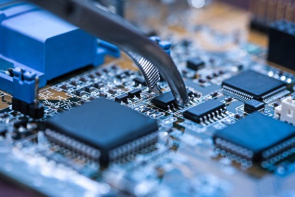
(Source:PMC)
To truly make the product stable, it also requires chip × packaging × circuit board to think together, which is what is called "co-design". In thermal design, the thermal path should be shortened and the TIM (Thermal Interface Material) and heat dissipation tube should be configured reasonably; in terms of electricity, the key signal should be shortest and the reflow path should be complete to avoid parasitic resistance, inductance, and capacitors affecting the signal quality; in the mechanism, the packaging thickness and tumbling must be controlled, otherwise the welding point will be uneven after re-welding, which is easy to cause problems in life tests. The sooner these things are, the more you can avoid rework and bad work in the later stages.
Why do you need to do such a reliable test? The answer is: the product must live for many years between "hot, cold, tide, dry, and shock". If the packaging absorbs water and the water expands rapidly during re-welding, it may cause damage as commonly known as "popcorn effect"; the heat expansion between the materials is inconsistent, and the layers will become corroded or disconnected over time; frequent temperature cycles and mechanical stress may also cause welding points to be exhausted and cracked. The standardized process is precisely to keep these risks under acceptable ranges.
From packaging to top board: Last mileAfter the packaging is completed, the finished product will be cut, selected and mounted on the loader (tape & reel) and sent to the SMT line. The paddle machine puts it at the designated position of the PCB, and melts the solder balls through re-welding, and finally use X-ray to check whether the solder points are full or not soldered. At this point, an IC is truly "on board" and becomes a reliable part in your mobile phone, home appliance or vehicle system. In terms of industry division, multiple volumes of product packaging are performed by professional packaging factories, such as Sun and Moonlight and Amkor; the system design will cooperate with them to adjust materials, heat dissipation and test plans.
The packaging handles the fragile bare crystal into standard parts that can be mass-produced, automatically disassembled, and can be used for a long time. For users, what really hits the market is not the "chip" itself, but the whole "chip + packaging".